Consider a 3-pole bandpass filter centered on 100 MHz with a ripple bandwidth of 5 MHz. According to M. Dishal, we only need two parameters to design the fundamental filter circuit shown below: end-loaded Q and coupling factor k12. In the equations named “Parameters” in the schematic below, care is also taken for converting the ripple bandwidth to the 3-dB bandwidth of the filter, needed for calculating the circuit elements. A choice is make for the resonator inductance. This is usually done on the basis of realisability and/or for obtaining maximum resonator-Q (lowest filter insertion loss). All other parameters are calculated from the two ‘k and Q’ parameters: q1 and k12 obtained from the tables in Anatol Zverev’s classic book.
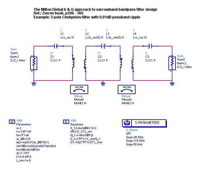
Note, that the sources are inserted into the end-resonators (The ADS circuit simulator uses a resistor symbol for a source with internal impedance). The internal source impedance follows from the end-loaded Q and the reactance of the resonant circuit elements. The normalised value of the end-loaded Q is 1.1811 – as given in the Zverev book. This lossless circuit may not be of practical value for a real filter design, but it illustrates the theoretical relationships.
The filter response graph below is valid for all filter realisations shown on this page. There is a noticeable asymmetry of the transmission factor S21. This asymmetry is due to the frequency dependency of the lumped element coupling elements. Insofar, the design is approximate and only valid for narrow bandpass filters (BW/fc < 10%).

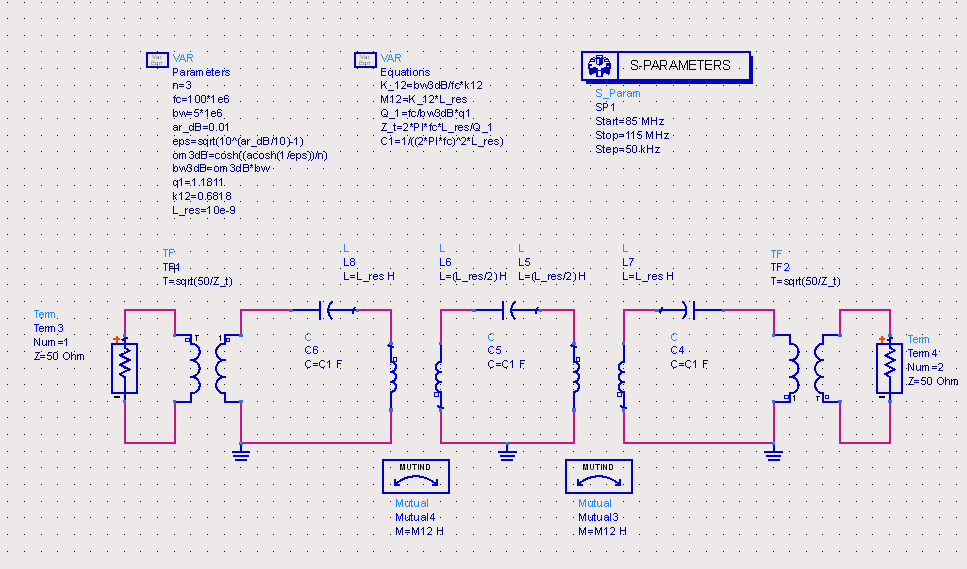
We can also use ports with standard impedances by employing ideal transformers. The transformer ratio is chosen to transform the standard source and load impedances to those required to produce the end-loaded Q (Z_t).
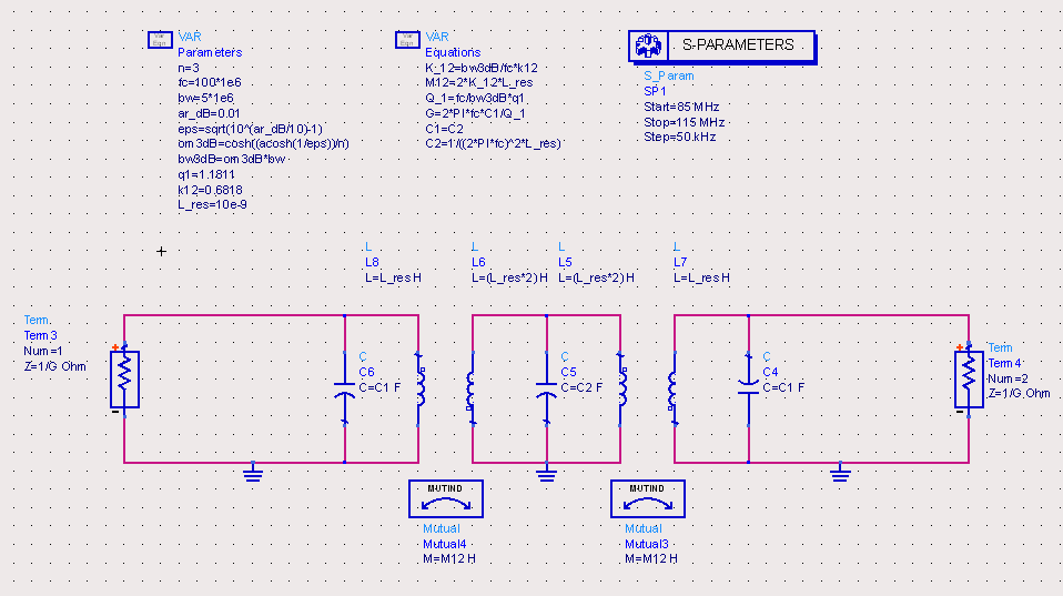
Instead of using resonator loops, shunt-type parallel tuned resonant circuits can be used as shown in the schematic below. Naturally, the port impedance is here very high and therefore not of practical value for most applications.
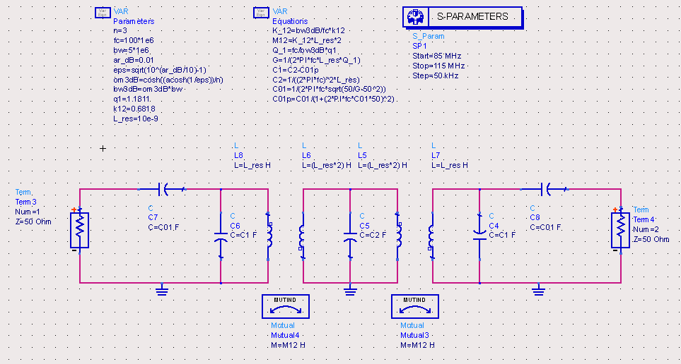
A suitable practical way of transforming the standard source and load impedances is used in the circuit below. The input- and output coupling circuit can be explained as follows: the series combination of the 50 Ohms source/load impedance and C01 – when transformed to its narrowband parallel equivalent – becomes 1/G as in the circuit above and the parallel capacitance becomes C01p (See “Equations” in the schematic below). In other words: a simple series-to-parallel conversion in the form Y = 1 / Z is the underlying principle. This principle is strictly only valid for use with narrowband filters, due to the frequency dependency of the impedance transformation.
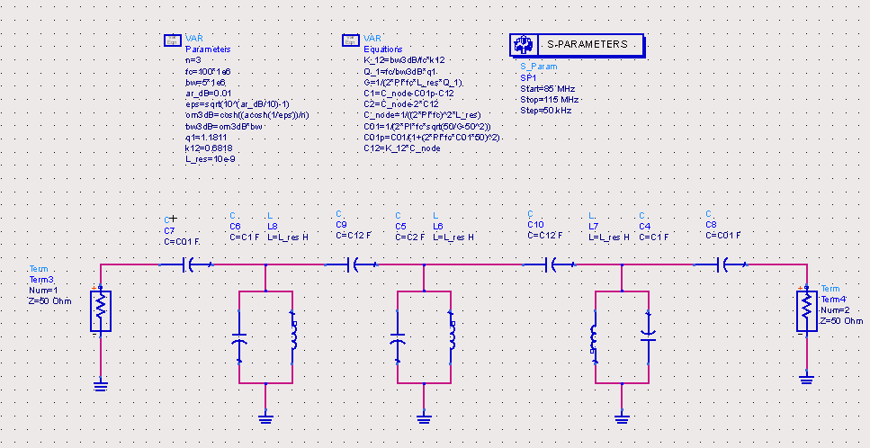
Finally, a very practical circuit is arrived at as shown below. The coupling k12 is now realised with capacitances C12. This narrow bandpass filter circuit is rather popular among filter designers as it uses a minimum number of inductances. Again, this design approach is only valid for narrowband filters.
The shown filter circuits illustrate that there are many ways of designing a lumped element filter for a given transfer function. The required couplings and end-loaded Q’s must exist – but there is a lot of freedom for realising them.
Note, that the resonator inductance can be chosen so as to suit practical considerations. The resonator capacitors are always calculated for the required nodal resonant frequency. Note, that the nodal resonance is determined by all three capacitors connected to a resonator node ( C_node_i = C_i + C_i-1_i + C_i_i+1, eg. C_node_1 = C1 + C01 + C12 ). Of course, the capacitor values must also remain within practical limits if the filter is going to be realised as a lumped element filter and this is of course determined by the chosen resonator inductance.