Planar filters are marked by having flat 2D-like resonators in the form of strips or patterns of strip elements usually located between metallic ground planes. They can insofar be regarded as another realisation method of TEM-mode filters where an electric field exists between a conductor and one or two ground planes with the magnetic field surrounding the “inner” conductor. While such filters may use air as a dielectric media, planar filters nowadays often use a solid dielectric upon which a metal filter circuit layer is placed with the main ground layer on the underside of the dielectric. The structure is therefore very similar to a printed circuit board. The major difference to a PCB is that the metal conductor pattern is designed to create resonators and to provide the required coupling relationships between the filter elements rather than just providing connections between parts soldered on to the PCB. The solid dielectric is often referred to as “substrate”, leaning on the word’s meaning in the sense of a printing process. Given the unsymmetrical cross-section of traditional substrate based stripline resonators (bottom metal ground, substrate, metal circuit layer, air, top metal ground), the fields surrounding the strip are in two different media, meaning that part of the field is in the substrate and another – usually a much smaller part – is in the air above the strip. The higher permittivity of the substrate (usually: Epsilon_r > 2.0) causes the E-field to concentrate in the substrate. Naturally, the losses due to this field concentration in a usually rather lossy substrate material are significant. Standard Expoxy-based material, like FR4 can be used below 1 GHz for filters with large relative bandwidth in certain cases. Teflon-based material is however the commonly used substrate for planar filters. Low loss and high permittivity (> 9.0) can be obtained from so-called “alumina” (Al2O3) ceramic materials but the cost penalty is high. It needs to be mentioned that PCB-type planar structures may show the effect of two different propagation types because the fields exist both in the dielectric material (under the conductor) as well as in air (above the conductor). Such layered dielectric effect can manifest itself in a variety of phenomena, but usually there is no impairment of the functionality of a microstrip planar filter.
Most planar filters using a solid dielectric are commonly known as “microstrip filters”, the word “micro” referring to the relatively thin metal strips used. “Microstrip” usually denotes a uniform width strip transmission line on a PCB (as shown below). “Microstrip filters” therefore often integrate conveniently into an overall PCB circuit. However, given that a major part of the electric field of a microstrip resonator exists inside a somewhat lossy dielectric material, the achievable unloaded quality factor values of microstrip resonators are usually below 1000. (In contrast to that: Coaxial TEM-mode resonators can have unloaded Q values of several 1000s). This is a major limitation of typical microstrip filters, especially if a relative narrow passband width is required. The thin strip conductor also sets a limitation on power handling. Heat transfer via the substrate is poor and most microstrip resonators are thermally rather isolated, limiting their use to low or moderate power levels.
The solid dielectric base material usually has a dielectric constant substantially greater than 1.0 and therefore the physical length of a microstrip resonator is a great deal shorter than that of a stripline resonator in air. While this may seem convenient in terms of size reduction, it comes with the additional penalty of increased current density. Consequently there are higher losses in the conductor material on top of the losses in the substrate.
A planar resonator
A commonly used planar microstrip resonator type is the “open-ended halfwave resonator” as shown below
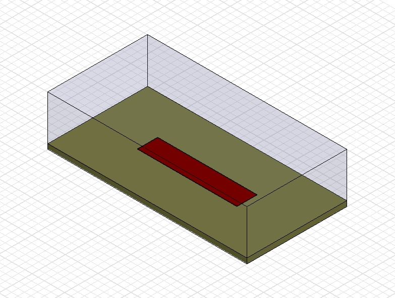
The copper strip is electrically half a wavelength long and has no metallic connection to the ground layer under the substrate material. “Electrically” here implies that the wavelength on a microstrip resonator is physically shorter than the free-space wavelength due to the larger capacitance per unit length introduced by the dielectric material under the strip. The width of the copper strip determines its characteristic impedance together with the Eps_r of the substrate. Unlike coaxial resonators in air, there is however, no distinct Q maximum at a particular value of the characteristic impedance. The reason for this unique microstrip resonator behavior is rather interesting: As the width of a microstrip resonator increases, the “active” substrate area (volume) under the strip also increases and the advantage of lower losses in the wider copper strip is by and large lost because of higher losses in the dielectric material. This phenomenon is illustrated in more detail here.
Similar to coaxial resonators, the abrupt ends of the strip cause strong E-field discontinuities which can be associated with an equivalent shunt capacitance loading the resonator at its ends and thereby further lowering the resonant frequency . In the case of the above shown resonator, the physical length of the strip is 30mm and its resonant frequency is 3.262 GHz. Had the strip conductor not been on a substrate (Eps_r = 2.3), but in air instead, the resonant frequency would be (299.79*10^8 m/sec)/(2 x 0.03m) = 5 GHz. The approximate length reduction of a microstrip resonator can be calculated via sqrt(Eps_r). In the given case, this would yield a resonator frequency of 5.0 / sqrt(2.3) = 3.297. The actual value (3.262 GHz) is a little lower due to the earlier mentioned end-effects.
3D electromagnetic simulation allows us to “see” the resonator’s E-field:
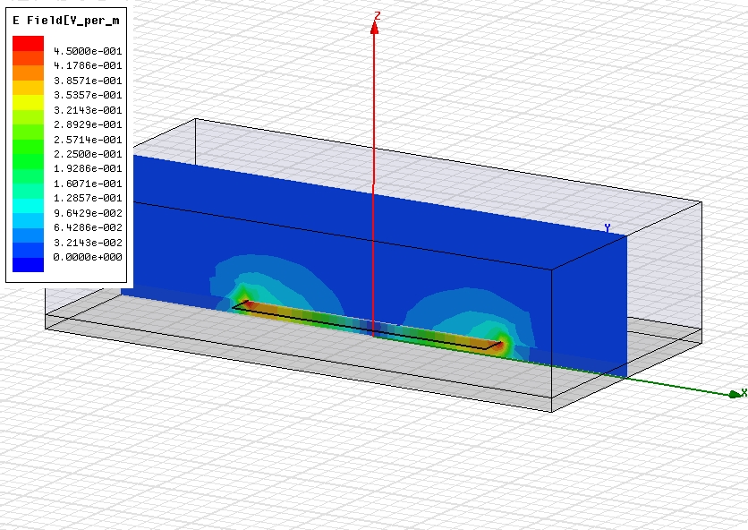
The E-field discontinuities are clearly visible in the form of strong field concentration at the two ends of the strip conductor. Field concentration within the substrate material under the strip conductor can also be detected by the rainbow colour pattern of the cross-sectional view above. If we plot the E and H-field magnitudes along a line halfway below the strip conductor inside the substrate, we can clearly see the normal sine and cosine behaviour of the fields of a halfwave long, open-ended transmission line resonator. Note, that the horizontal axis of the graph is distance from one end of the box (shown above) and therefore the center of the graph is to be taken as x=0.
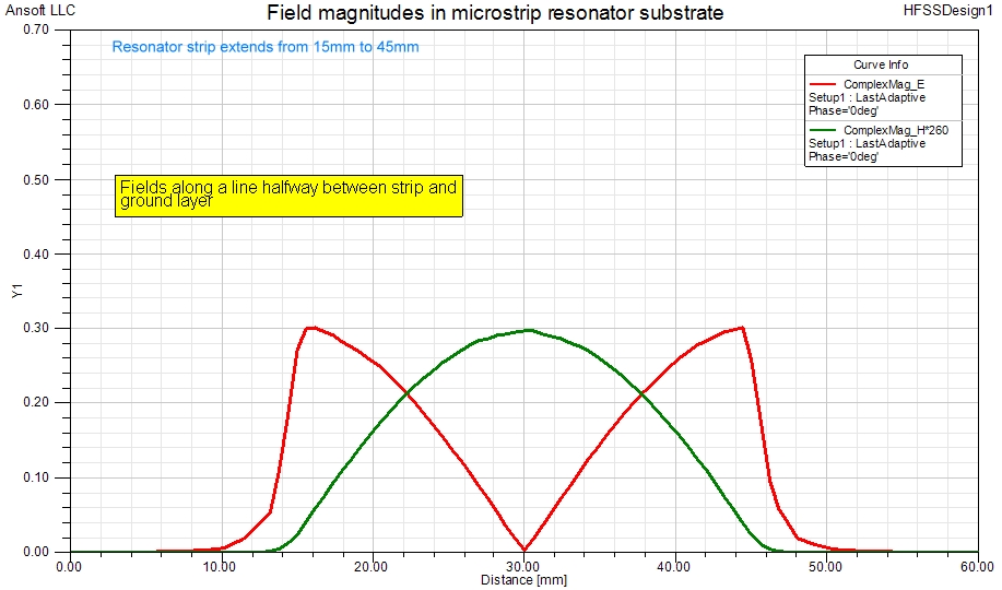
The earlier mentioned end discontinuities cause a visible departure from the typical sine function behavior (-pi/2 to pi/2 with x=0 at 30mm) of the electric field magnitude (red) at both ends of the resonator. There the E-field magnitude drops abruptly but does not reach zero directly. The cosine function H-field magnitude behavior (green) is also affected by the discontinuity, seen as a rounding of the curve near the resonator strip ends.
Finding the resonator parameters
The two most important parameters of a filter resonator are its resonant frequency and its quality factor – usually referred to as “unloaded quality factor”. (“unloaded” here means that the quality factor is entirely dependent upon the losses in the resonator – not on any external resistive loading.) Eigenmode simulation will provide us with these two parameters (and with all higher mode resonances and associated Q’s). In the case of the above shown halfwave microstrip resonator the values are: f_res = 3262 MHz and Qu = 607.
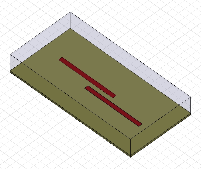
If Eigenmode simulation is not available, the so-called “light coupling method” can be used as shown below. In order to enable transmission through a resonator, the ends of the resonator are lightly coupled to two ports via short lines utilising electrical field coupling (capacitive coupling). Looking at the response plot (2nd image below), this structure essentially resembles that of “a badly designed 1-pole bandpass filter” having much too weak couplings and consequently a very high insertion loss due to excessive mismatch.
Driven mode simulation will typically yield a transmission response that looks like the one shown below. Maximum transmission occurs at resonance (l_e = λ/2). Some gap size iteration and sweep range iteration may be required during the simulation work.
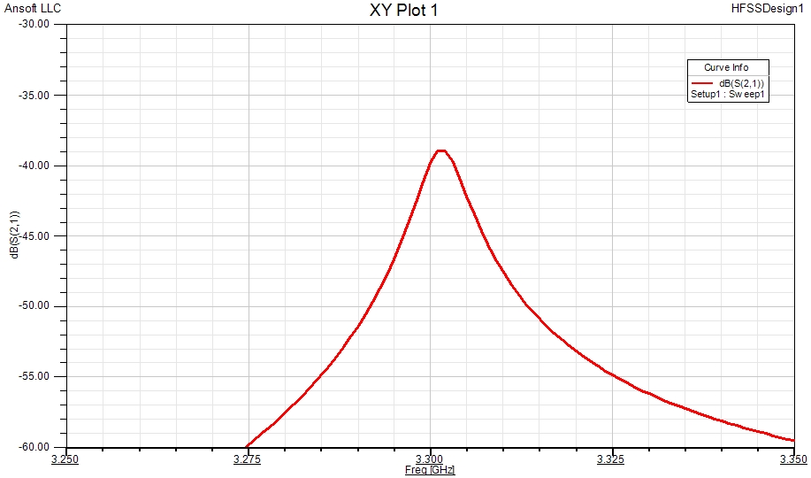
The transmission peak occurs at the resonant frequency – with a minor shift caused by the capacitive loading from the two port coupling strips. The transmission peak is at -40 dB indicating that the coupling is “light” and not causing excessive loading of the resonator. The thus found resonant frequency is 3301.5 MHz – only deviating by +1.3% from the more accurate Eigenmode simulation result. If the material constants are defined properly, we can also find the unloaded Q with relatively good accuracy by locating the -3dB points relative to the S21 peak value on the graph below. For this purpose, a narrow and finer sweep around the resonance peak is advantageous:
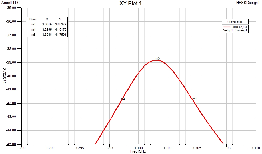
We find the resonator Q by dividing the resonance peak frequency (m3) through the difference of the -3dB frequency points (markers m4, m5): 3.3015 / (3.3046 – 3.2985) = 541. The difference to the more accurate Eigenmode simulation result (Qu=607) is only -12.3%.
Coupling between resonators
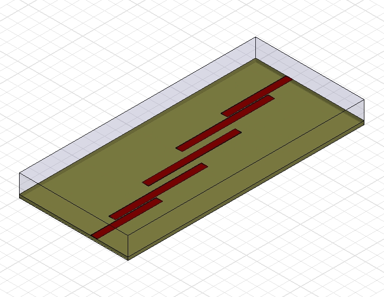
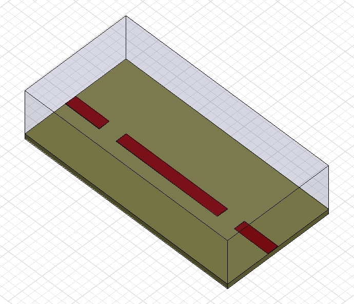
There are many ways to create coupling between microstrip resonators. Traditionally, the principles of coupled lines are followed, leading to parallel sub-sections of two resonators as shown below.
A more general approach to the design of couplings in microstrip filters is possible when 3D electromagnetic simulation is used. It is then for example not necessary to have impedance steps in the resonators strips as is often seen in more traditional microstrip filter designs. The impedance steps are perhaps more a consequence of an early design process rather than a necessity for the filter structure.
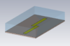
The two halfwave long resonators in the picture below can be subdivided into one middle section consisting of coupled lines and two transmission line (un-coupled) end sections. Maximum coupling is achieved when the middle section is a quarter of a wavelength long – a principle well-known from the theory of directional couplers. The strength of the coupling depends mainly on the gap between the metal strips (in terms of coupled line theory: the odd-mode impedance, Zoo).
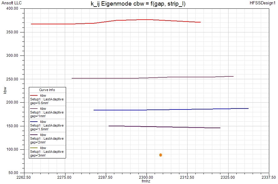
Advantageously, the coupling design can be done by using Eigenmode simulation. The graph below shows the results of such simulation for various gap widths and with a minor sweep of the strip lengths so as to also see the frequency dependency of the coupling.
If Eigenmode simulation is not available, the earlier mentioned “light coupling technique” can also be used for the simulation of coupling between microstrip resonators. The two resonators are very lightly coupled capacitively to two short strips forming the conductor of rectangular microstrip ports.
A CST simulation data file which directly provides the coupling between two microstrip resonators can be obtained here.
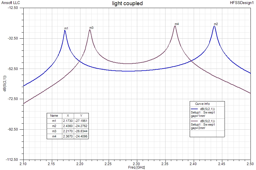
The two Eigenmodes are resonances at distinct frequencies and at those frequencies, a transmission peak must exist. The frequency location of the peaks then gives us the coupling strength – expressed here as the coupling bandwidth cbw. Therefore, we can obtain the coupling bandwidth directly from the graph above: gap = 1mm, cbw = (2436 – 2173)MHz = 263 MHz and for gap = 2mm, cbw = (2367 – 2217)MHz = 150 MHz. These values compare well with the Eigenmode results for the obtained earlier. Note, that a simplified formula for the relationship between the transmission peak frequencies and the coupling bandwidth has been used here.
Input and output coupling design
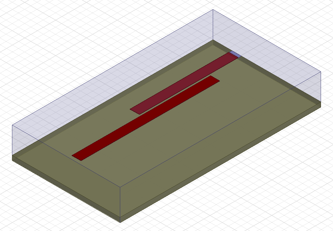
The input and output couplings of a microstrip filter are designed – like in any other coupled-resonator filter – to produce the required loaded quality factors (called: Q_end or Q_e) in the outermost resonators. The Q_end is determined by the strength of the coupling between source/load impedance and the end-resonator. The stronger the coupling, the lower the Q_end. For the design we need to be able to obtain the Q_end and resonator frequency from simulation and the easiest way is to use Eigenmode simulation. The structure shown below is used for that purpose. It contains the end-resonator and the coupling to the filter port in the form of a stripline with a narrow gap to the halfwave-resonator. As HFSS does not allow ports in Eigenmode simulation (CST does!), I placed a small 2D element at the outer end of the coupling strip. A lumped-RLC boundary is then defined across the 2D element. The RLC boundary is defined as R = input stripline characteristic impedance. The latter was determined by 2D simulation of the cross-section.
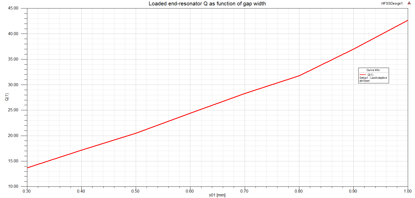
The gap width can be swept in a parametric sweep so as to get the curve below showing the relationship between Q_end and the gap width. Clearly with increasing gap width, the Q_end increases because the coupling between the coupling strip and the resonator decreases.
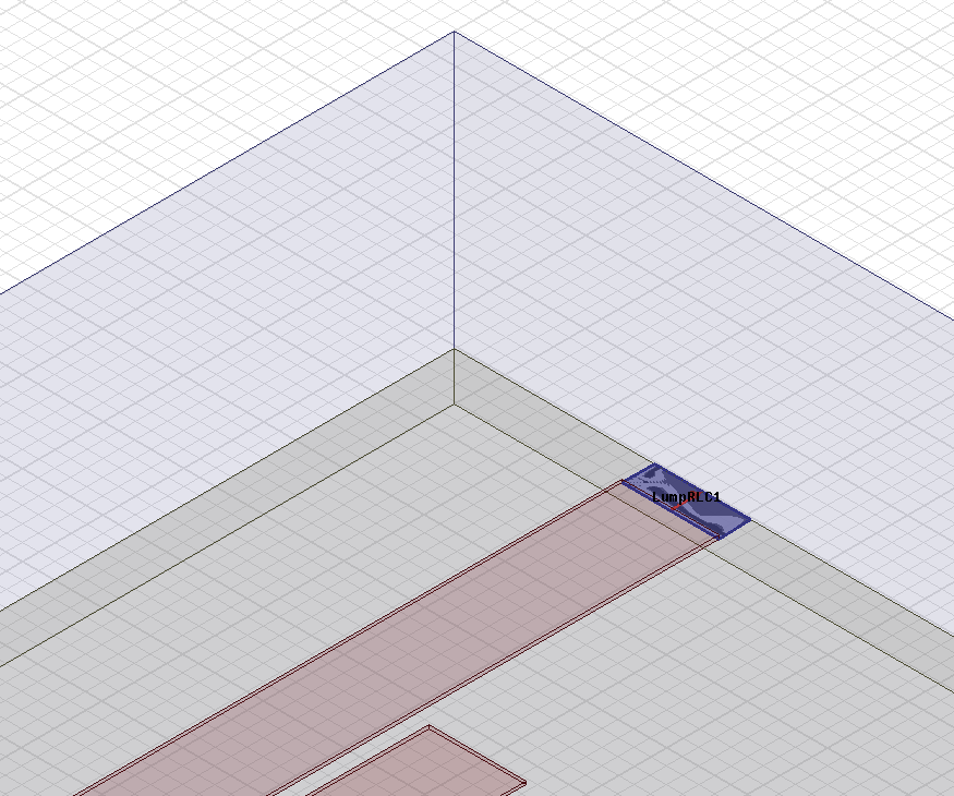
The RLC boundary can be seen in more detail in the image below.
By adjusting the resistive loading of the end-resonators via a suitable impedance transformation we achieve the loaded-Q that is pre-determined by the desired filter response (coupling matrix data).
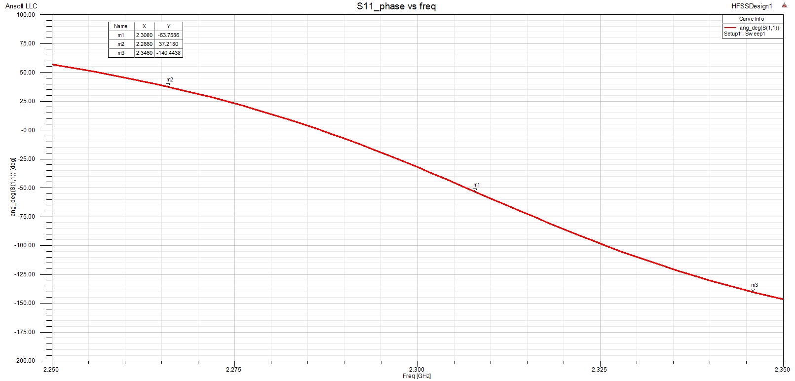
If Eigenmode simulation is not available, the Q_end can also be found from driven-mode simulation as shown below. We use the S11-phase response for that purpose. Due to the absence of any internal resistive component, there is total reflection but the Q_end can be extracted from the S-11 phase response:
Q_end = ω0 / ( Δω_+-90° )
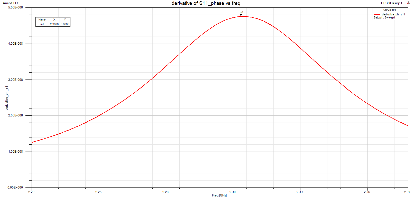
Frequency markers are placed in the S11-phase response at f_res and at the +/- 90° points with reference to the S11-phase at the resonance point. The resonant frequency can be found accurately by plotting the derivative of S11-phase vs frequency. This is shown in the 2nd graph below.
On the basis of the above coupling graphs together with the nominal filter coupling data, the overall filter simulation model can be “constructed”. Fine-tuning of the resonators and fine-adjustment of the coupling gaps will always be required. The usual approaches involving optimisation and parameter extraction (space mapping) apply. It is important to use an equation-based simulation geometry model where all dimensional relationships are taken care of by suitable formulas rather than using numbers for dimensional data.
– to be continued –
Hi,
could you provide a simple example how eigenmode analysis of a microstrip resonator works using CST?
Hi Oliver,
Sorry for the delay. I was flooded with work but I’ll send you an example directly to your e-mail address today or tomorrow.
best wishes
Dieter
rfcurrent.com